
Glass Interposer: The Foundation of Next-Generation Semiconductor Packaging
The semiconductor industry is entering a new era where package architecture is becoming as critical as transistor scaling. As artificial intelligence (AI), high-performance computing (HPC), advanced networking, and silicon photonics demand greater bandwidth and functionality, manufacturers are increasingly adopting chiplet-based architectures that integrate multiple specialized semiconductor dies into a single package.
Connecting these chiplets efficiently requires a sophisticated interconnect platform capable of supporting thousands of high-speed electrical connections while maintaining signal integrity and manufacturing precision. This is where the glass interposer has emerged as a transformative technology.
By combining excellent electrical performance, dimensional stability, and scalable manufacturing, glass interposers are enabling the next generation of heterogeneous semiconductor integration.
What Is a Glass Interposer?
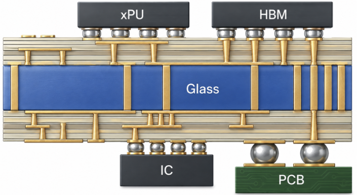
Glass interposer redistributes high-density electrical signals, power, and ground connections while providing mechanical support for multiple integrated circuits within a single package.
Unlike conventional package substrates, glass interposers support extremely fine redistribution layers (RDLs), dense vertical interconnects, and precise alignment across large package areas. This enables processors, memory, RF devices, photonic integrated circuits, and other specialized chiplets to communicate with exceptionally high bandwidth and low latency.
As heterogeneous integration becomes the preferred design approach across the semiconductor industry, glass interposers are becoming a key enabling technology for advanced package architectures.
Why Modern Semiconductor Packages Need Glass Interposers
For decades, semiconductor performance improvements came primarily from transistor scaling. Today, innovation increasingly comes from combining multiple optimized chiplets into a single package.
Instead of manufacturing one very large processor, designers can integrate compute dies, High Bandwidth Memory (HBM), RF components, photonic devices, and specialized accelerators using advanced packaging techniques. This modular approach improves manufacturing yield, shortens development cycles, and allows each die to be fabricated using the most appropriate process technology.
The success of this architecture depends on the interposer. It must route thousands of high-speed connections while maintaining low latency, reliable power delivery, and excellent signal integrity. As package complexity continues to increase, glass has become an attractive platform for supporting these demanding requirements.
Why Glass?
Glass provides several advantages that make it well suited for advanced semiconductor packaging.
Its electrically insulating nature reduces substrate losses while supporting excellent signal integrity at high frequencies. The exceptional dimensional stability of glass enables precise alignment throughout manufacturing, supporting increasingly fine redistribution layers and dense interconnect structures. Its smooth surface also facilitates high-resolution lithography and uniform metal deposition.
Unlike organic substrates, which face challenges as routing density increases, glass provides a pathway toward increasingly complex package architectures. Compared with silicon, glass offers lower electrical losses and is compatible with scalable panel-level manufacturing approaches that may improve production efficiency as adoption grows.
Through Glass Vias: Enabling High-Density Integration
Many glass interposers incorporate Through Glass Vias (TGVs) to create vertical electrical connections through the substrate. TGVs allow signals, power, and ground to transition efficiently between routing layers while maintaining excellent electrical performance.
The insulating properties of glass help reduce parasitic capacitance and substrate losses, making TGV technology particularly attractive for RF, millimeter-wave, and high-speed digital applications.
For a deeper discussion of TGV fabrication, materials, and design considerations, read our dedicated article on Through Glass Via (TGV) Technology.
Supporting AI, HBM, and Chiplet Architectures
Artificial intelligence has dramatically increased the performance requirements placed on semiconductor packages. Modern AI accelerators often integrate multiple compute chiplets alongside several stacks of High Bandwidth Memory (HBM), creating thousands of parallel electrical connections operating at extremely high data rates.
Glass interposers provide the routing density, dimensional precision, and electrical performance needed to support these advanced package architectures. As memory bandwidth and chiplet counts continue to grow, glass interposers are expected to play an increasingly important role in enabling future AI platforms.
Beyond Interconnects: A Platform for Advanced Integration
Glass interposers are evolving beyond simple routing substrates.
They can also support the integration of passive RF structures—including inductors, capacitors, transmission lines, baluns, and filters—within the substrate itself. Combining routing and passive integration reduces component count, shortens signal paths, and enables more compact System-in-Package (SiP) solutions.
This capability is particularly valuable for RF front ends, phased-array antennas, satellite communications, and emerging silicon photonics applications.
The Future of Glass Interposer Technology
As semiconductor innovation increasingly shifts from transistor scaling to advanced packaging, the importance of the interposer will continue to grow. Future semiconductor systems will integrate compute, memory, RF, photonics, sensors, and passive components into highly optimized heterogeneous packages.
Glass interposers provide the routing density, electrical performance, and manufacturing precision needed to support this evolution. Their compatibility with chiplet architectures, AI accelerators, advanced RF systems, and co-packaged optics positions them as a foundational technology for the next generation of semiconductor packaging.
Why 3D Glass Solutions?
3D Glass Solutions develops advanced glass technologies that enable next-generation semiconductor packaging through proprietary glass processing, Through Glass Via (TGV) technology, and integrated passive device (IPD) solutions. By combining materials innovation with advanced manufacturing, we help customers develop high-performance packaging solutions for AI, RF communications, silicon photonics, aerospace, defense, and other demanding applications.